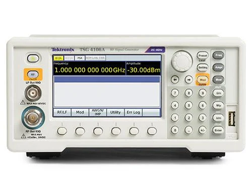

TSG4100A 벡터신호발생기
| 주파수 범위 | 950 kHz to 2/4/6 GHz |
|---|---|
| 출력 파워 | -110 dBm to +16.5 dBm |
| 위상 잡음 | -124 dBc |
| IQ대역폭 | 최대 6 MHz |
TSG4100A 시리즈 벡터신호발생기
TSG4100A 시리즈 RF 벡터 신호 발생기는 중간급 RF 성능과 최대 200MHz의 변조 대역폭을 제공합니다. 편리한 현장 내 소프트웨어 업그레이드를 통해 아날로그에서 고급 벡터 및 디지털 변조 기능으로 장치를 손쉽게 전환할 수 있으므로, 매우 유연한 구성과 최고의 CAPEX 보호를 사용할 수 있습니다.
특징 |
장점 |
| 최대 6MHz의 내부 IQ 대역폭 | 출력 기본 디지털 RF 신호 및 좁은 대역폭 통신 신호. |
| 최대 200MHz의 외부 IQ 대역폭 | 무선/통신 신호를 위한 매우 넓은 대역폭 |
| 소프트웨어를 통해 내부 벡터 변조 소스로 손쉽게 업그레이드 | 아날로그 및 벡터 신호 발생기 애플리케이션을 모두 매우 저렴한 비용으로 사용할 수 있습니다. |
| OCXO 시간 기반이 | R&D 애플리케이션을 위한 탁월한 수명 및 안정성 성능 |
| 출력 주파수 범위가 트루 DC에서 시작합니다. | DC/저주파수 애플리케이션을 위한 기타 장비를 추가할 필요가 없습니다. |
| 모델 | 현장 내 업그레이드 가능 옵션 | 주파수 범위 | 정가 |
|---|---|---|---|
| TSG4102A | 기본 벡터 변조, GSM, EDGE, P25, W-CDMA, DECT, NADC, PDC, TETRA, 오디오 분석, 외부 IQ 변조 |
2GHz |
₩11,300,000 |
| TSG4104A | 기본 벡터 변조, GSM, EDGE, P25, W-CDMA, DECT, NADC, PDC, TETRA, 오디오 분석, 외부 IQ 변조 |
4GHz |
₩14,600,000 |
| TSG4106A | 기본 벡터 변조, GSM, EDGE, P25, W-CDMA, DECT, NADC, PDC, TETRA, 오디오 분석, 외부 IQ 변조 |
6GHz |
₩21,500,000 |
Specifications
All specifications are guaranteed unless noted otherwise. All specifications apply to all models unless noted otherwise.
Frequency
- BNC output, all models
- DC to 62.5 MHz
- N-type outputs
-
- TSG4102A
- 950 kHz to 2.0 GHz
- TSG4104A
- 950 kHz to 4.0 GHz
- TSG4106A
- 950 kHz to 6.0 GHz
- Frequency resolution
- 1 μHz at any frequency
- Switching speed
- <8 ms (to within 1 ppm)
- Frequency error
- <(10–18 + time-base error) × fc
- Frequency stability
- 1 × 10–11 (1 s Allan variance)
Front panel BNC output
- Frequency range
- DC to 62.5 MHz
- Amplitude
- 1.00 VRMS to 0.001 VRMS (-47 dBm to +14.96 dBm)
- Offset
- ±1.5 VDC
- Offset resolution
- 5 mV
- Maximum excursion
- 1.817 V (amplitude + offset)
- Amplitude resolution
- <1 %
- Amplitude accuracy
- ±0.7 dB
- Harmonics, typical
- <–40 dBc
- Spurious, typical
- <–65 dBc
- Output coupling
- DC, 50 Ω ±2%
- Impedance
- 50 Ω
- Reverse protection
- ±5 VDC
- VSWR, typical
- < 1.6 :1
Front panel N-type output
- Power output
-
- TSG4102A
- +16.5 dBm to –110 dBm
- TSG4104A
- +16.5 dBm to –110 dBm (<3 GHz)
- TSG4106A
- +16.5 dBm to –110 dBm (<4 GHz)
+10 dBm to –110 dBm (4-6 GHz)
- Voltage output
-
- TSG4102A
- 1.5 VRMS to 0.7VRMS
- TSG4104A
- 1.5 VRMS to 0.7 μVRMS (<3 GHz)
- TSG4106A
- 1.5 VRMS to 0.7 μVRMS (<4 GHz)
- Amplitude resolution
- 0.01 dBm
- Amplitude accuracy
-
- CW, 50 Ω load (dB, typical)
-
CW, 18 °C to 28 °C >10 dBm 10 to -30 dBm -30 to -60 dBm -60 to -100 dBm <-100 dBm 10 MHz to 0.1 GHz ±0.2 ±0.25 ±0.35 ±0.45 ±0.6 0.1 GHz to 2 GHz ±0.15 ±0.15 ±0.25 ±0.35 ±0.6 2 GHz to 4 GHz ±0.3 ±0.2 ±0.35 ±0.6 ±0.8 4 GHz to 6 GHz NA ±0.3 ±0.4 ±0.75 ±1.25 - CW, 50 Ω load (dB, max)
-
Level range: +5 to -30 dBm (max) +5 to -30 dBm (typical) Temperature: 18 °C to 28 °C 5 °C to 40 °C 5 °C to 40 °C 10 MHz to 0.1 GHz ±0.6 ±1.0 ±0.7 0.1 GHz to 2 GHz ±0.6 ±1.0 ±0.6 2 GHz to 4 GHz ±0.6 ±1.0 ±0.7 4 GHz to 6 GHz ±1 ±1.5 ±0.9
- Impedance
- 50 Ω
- Output coupling
- AC, 50 Ω
- VSWR, typical
- <1.5 (2 MHz to 2 GHz)
<1.8 (2 GHz to 6 GHz)
- Reverse protection
- 30 VDC, +25 dBm
- IQ modulation output level accuracy
- Output amplitude is -5 dBm.
Temperature: 18 °C to 28 °C 5 °C to 40 °C Fc: Typical (dB) Max (dB) Typical (dB) <2 GHz ±0.1 ±0.4 ±0.4 2 GHz to 4 GHz ±0.2 ±0.6 ±0.4 4 GHz to 6 GHz ±0.4 ±0.8 ±0.7
Spectral purity of the RF output
- Subharmonics
- None
- Harmonics, maximum
- Output level <0 dBm, 1 GHz CW signal
- TSG4102A and TSG4104A
- < -38 dBc
- TSG4106A
- < -30 dBc
- Harmonics, typical (output level < 0 dBm)
- < -35 dBc, CW , Fc < 2 GHz
- Spurious (typical)
- Output level -10 dBm, CW
- < -68 dBc
- < -55 dBc
- Residual FM, typical
- 1 Hz rms (300 Hz to 3 kHz bandwidth)
- Residual AM, typical
- 0.006 % rms (300 Hz to 3 kHz bandwidth)
- SSB phase noise
- Output level is +5 dBm at 18 °C to 28 °C.
Carrier <th class="cellrowb 1 kHz 10 kHz 20 kHz 1 MHz 1 GHz -102 -110 -113 -124 2 GHz -96 -104 -107 -118 3 GHz -93 -102 -105 -120 6 GHz -87 -96 -99 -114
- SSB phase noise at 1 GHz carrier, maximum (output level +5 dBm, 5 ℃ to 40 ℃)
-
- 1 kHz offset
- –95 dBc/Hz
- 10 kHz offset
- –106 dBc/Hz
- 20 kHz offset
- –107 dBc/Hz
- 1 MHz offset
- –120 dBc/Hz
- 2 GHz offset
- –118 dBc/Hz
- >3 GHz offset
- –120 dBc/Hz
Hardware options (All regions except North America)
Options M00 or M01 must be specified at the time of instrument order.
- M00
- Instrument with oven-controlled crystal oscillator (OCXO)
- M01
- Instrument with voltage-controlled crystal oscillator (VCXO)
- GPIB
- Adds GPIB interface
Hardware options (North America only)
Option E1 must be specified at the time of instrument order.
- E1
- Instrument with oven-controlled crystal oscillator (OCXO) time-base and GPIB interface
Hardware options (All regions)
- TSG4100A-RM1
- Single rack mount kit (can be ordered separately)
- TSG4100A-RM2
- Dual rack mount kit (can be ordered separately)
- TSG4100A-ATT
- 30 dB, 5 W RF attenuator up to 6 GHz
- D1
- A list of performance verification test results
Software options
To upgrade to vector/digital modulation capability and/or add more modulation options after initial purchase, order "TSG4100A-UP + VM xx” instead of “TSG410xA VMxx”.
- VM00
- Basic vector modulation package with internal 6 MHz modulation bandwidth
- VM01
- GSM modulation (requires Option VM00)
- VM02
- GSM EDGE modulation (requires Option VM00)
- VM03
- W-CDMA modulation (requires Option VM00)
- VM04
- APCO-25 modulation (requires Option VM00)
- VM05
- DECT modulation (requires Option VM00)
- VM06
- NADC modulation (requires Option VM00)
- VM07
- PDC modulation (requires Option VM00)
- VM08
- TETRA modulation (requires Option VM00)
- VM10
- Audio Clip (analog AM and FM)
- EIQ
- External 200 MHz modulation bandwidth (requires Option VM00)
INFORMATION
상호 : 주식회사 알트로닉스 주소 : 서울특별시 금천구 가산디지털2로 101, 한라원앤원타워 B동 1401호 Tel : 02-2101-2140 Fax : 02-2101-2142
사업자등록번호 : 292-88-01789
사업자등록번호 : 292-88-01789
Copyright © 2019 주식회사 알트로닉스. All Rights Reserved.
designed by website.co.kr